Board Description
The LimeSDR X3 development board provides a hardware platform for developing and prototyping high-performance and logic-intensive digital and RF designs using and Xilinx FPGA and Lime Microsystems transceiver. For more information on the following topics, refer to the respective documents:
LimeSDR X3 board features:
RF transceivers
3x Lime Microsystems LMS7002M
Baseband ADCs
4x ADS424, Dual-Channel, 14-bit, 160Msps, Analog-To-Digital converter
Baseband DACs
2x MAX5878, Dual-Channel, 16-bit, 250Msps, Digital-To-analog converter
FPGA Features
Xilinx Artix-7 XC7A200T in 676-FCBGA (27x27) package
215,360 logic elements
740 DSP slices
13 Mb block RAM
x4 Gen 2 PCIe interface
10 clock management tile (CMT), each containing one MMCM and one PLL
FPGA Configuration
JTAG mode configuration
Memory Devices
256 Mbit FPGA configuration FLASH
4x 128Kbit (16K x 8) EEPROM (for each RF transceiver and FPGA data)
Other Devices
Temperature sensor
Crypto Authentication Device
GNSS receiver
Connections
Coaxial RF (SMA and uFL/MMCX) connectors
uFL/MMCX connectors and headers for reference clock IN/OUT, GNSS antenna
12V 6 pin PICe power connector
12V header for powering external devices
Fan headers
FPGA JTAG connector (2mm pitch)
Clock System
30.72MHz (default) VCOCXO and 38.4MHz (optional) VCTCXO
Possibility to use GNSS PPS signal as a reference when tuning VCOCXO frequency
Possibility to tune VCOCXO by Phase detector’s charge pump (to match a reference clock input) or by onboard DAC.
Possibility to synchronize multiple boards using CLK_IN and CLK_OUT headers or coaxial connectors.
Clock generator/PLL for baseband DACs, ADCs
Hardware for White Rabbit Precision Time Protocol (PTP) implementation
User I/O
2x PMOD headers (0.1” pitch) connected to FPGA
4x dual color (RG) LEDs connected to FPGA
4x Switches connected to FPGA
Board Size without connectors 232,5mm x 106,7mm (9.15” x 4.2”)
LimeSDR X3 board overview
The heart of the LimeSDR X3 board is Xilinx Artix-7 XC7A200T. Its main function is to transfer digital data between the PC and the board via the PCIe interface. The block diagram for LimeSDR X3 v1.0 board is as shown in Figure 1.
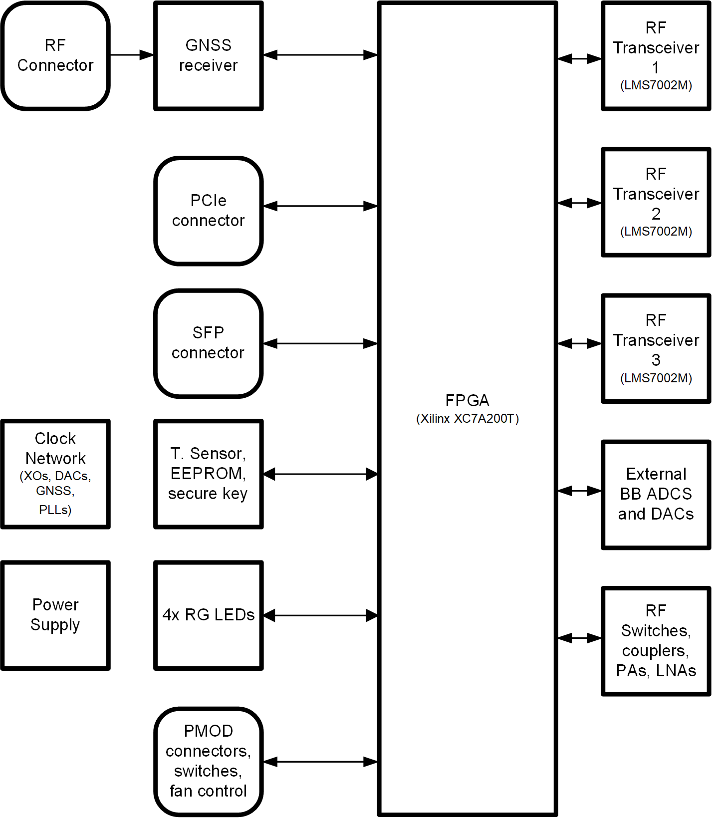
Figure 1. LimeSDR X3 v1.0 Board Block Diagram
LimeSDR X3 v1.0 board view with highlighted major components and connectors is presented in Figure 2 and Figure 3. Lime Microsystems LMS7002M RF transceivers, Xilinx Artix-7 FPGA and other main components are placed on the top side of the board. There are three connector types – data and debugging (PCIe x4, PMOD and JTAG), coaxial (clock input/output, GNSS antenna, RF transmit and receive ports), miscellaneous (fan headers).
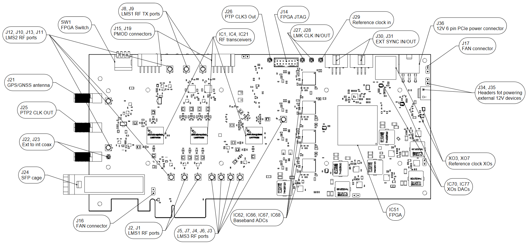
Figure 2. LimeSDR X3 v1.0 top side components and connectors
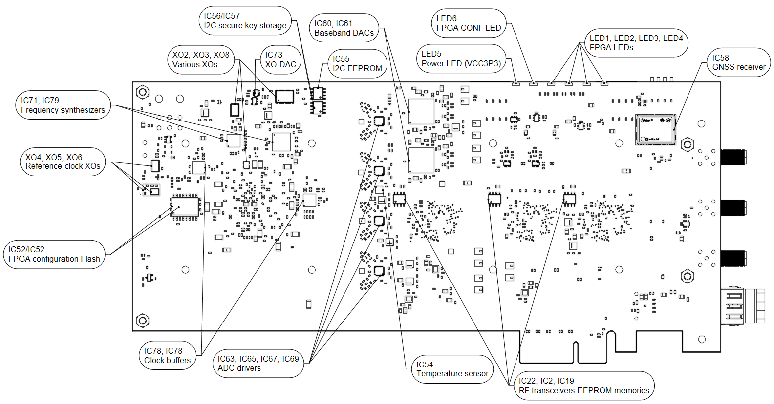
Figure 3. LimeSDR X3 v1.0 bottom side components and connectors
Board components description is listed in Table 1 and Table 2.
Featured Devices |
||
|---|---|---|
Board Reference |
Type |
Description |
IC1, IC4, IC21 |
RF transceiver |
Lime Microsystems LMS7002M |
IC51 |
FPGA |
Xilinx Artix-7 XC7A200T in 676-FCBGA (27x27) package |
IC62, IC64, IC66, IC68 |
Baseband ADC |
14-bit, 160 MSPS, ADS4246 |
IC60, IC61 |
Baseband DAC |
16-bt, 250 MSPS, MAX5878 |
IC58 |
GNSS module |
GNSS receiver LYNQ N20B |
Miscellaneous devices onboard |
||
Board Reference |
Type |
Description |
IC54 |
IC |
Temperature sensor LM75 |
IC56, IC57 |
IC |
I2C secure key storage ATECC508A |
IC63, IC65, IC67, IC69 |
ADC driver |
ADC driver ADA4930-2 |
Configuration, Status and Setup Elements |
||
Board Reference |
Type |
Description |
J14 |
JTAG chain pin header |
FPGA programming pin header for Xilinx platform cable. |
LED1, LED2, LED3, LED4 |
Red-green status LEDs |
User defined FPGA indication. |
LED5 |
Green status LED |
VCC3P3 power rail indication |
LED6 |
Red-green status LED |
FPGA init indication. |
General User Input/Output |
||
Board Reference |
Type |
Description |
J15, J19 |
Pin header |
2x PMOD connectors (8 FPGA GPIOs + 4 power pins, 0.1” pitch) |
SW1 |
Switch |
4-bit FPGA switch |
Memory Devices |
||
Board Reference |
Type |
Description |
IC2, IC19, IC22 |
EEPROM |
128K (16K x 8) EEPROM connected to each LMS7002M |
IC55 |
EEPROM |
128K (16K x 8) EEPROM connected to FPGA |
IC52/IC53 |
Flash memory |
FPGA configuration Flash (128 or 256 Mbit) |
Clock Circuitry |
||
|---|---|---|
Board Reference |
Type |
Description |
XO3 |
VCOCXO |
30.72 MHz voltage-controlled, oven controlled crystal oscillator used as a reference clock (connected by default). |
XO4-XO7 |
VCTCXO |
Various VCTCXOs (30.72 MHz, 38.40 MHz, 40.00MHz) voltage-controlled, temperature compensated crystal oscillators used as a reference clock (not connected by default). |
IC79 |
Clock generator |
Texas Instruments CDCM6208 |
IC74, IC78 |
Clock buffer |
Texas Instruments LMK00101 |
IC76 |
Phase detector |
Analog devices ADF4002, used to synchronize reference clock to external clock |
IC77 |
DAC |
16 bit DAC for XO VC tuning |
J29 |
U.FL/MMCX |
Reference clock input for phase detector (default) |
J27 |
U.FL/MMCX |
Clock input (LMK1_CLK1_IN) (not connected by default) |
J28 |
U.FL/MMCX |
Clock output (LMK1_CLKOUT) |
J30 |
6 pin header |
External synchronization input |
J31 |
6 pin header |
External synchronization output |
Precision Time Protocol (White Rabbit) hardware |
||
Board Reference |
Type |
Description |
IC70, IC73 |
DAC |
16 bit DAC for XOs VC tuning |
XO1 |
VCTCXO |
25 MHz VCTCXO |
XO2 |
VCXO |
20 MHz VCXO |
IC71 |
Clock generator |
Texas Instruments CDCM61004 |
J24 |
SFP cage |
SFP cage |
J25 |
SMA |
PTP clock output PTP_CLK2_OUT (from FPGA) |
J26 |
U.FL/MMCX |
PTP clock output PTP_CLK3_OUT (from FPGA) |
RF connectors |
||
Board Reference |
Type |
Description |
J1 |
U.FL/MMCX |
LMS1 RX1 port |
J2 |
U.FL/MMCX |
LMS1 RX2 port |
J3 |
U.FL/MMCX |
LMS3 TX2_2 port |
J4 |
U.FL/MMCX |
LMS3 RX1_W port |
J5 |
U.FL/MMCX |
LMS3 RX2_W port |
J6 |
U.FL/MMCX |
LMS3 RX1_H port |
J7 |
U.FL/MMCX |
LMS3 RX2_H port |
J8 |
SMA |
LMS1_TX1 port |
J9 |
SMA |
LMS1_TX2 port |
J10 |
U.FL/MMCX |
LMS2 TRX1 port |
J11 |
U.FL/MMCX |
LMS2 RX1 port |
J12 |
U.FL/MMCX |
LMS2 TRX2 port |
J13 |
U.FL/MMCX |
LMS2 RX2 port |
J21 |
SMA |
GNSS module active antenna connector |
J22 |
SMA |
External SMA to internal U.FL/MMCX |
J23 |
U.FL/MMCX |
|
Power Supply |
||
Board Reference |
Type |
Description |
J34 |
Pin header |
12V header for powering external devices (0.2” pitch) |
J35 |
Pin header |
12V header for powering external devices (0.1” pitch) |
J36 |
6 pin PCIe power |
12V PCIe power connector for powering board |
Other |
||
Board Reference |
Type |
Description |
J16, J17, J18 |
Header |
Fan connection headers. Selectable voltage 3.3V, 5V or 12V (5V default). |
LimeSDR X3 board architecture
More detailed description of LimeSDR X3 board components and interconnections is given in the sections of this chapter.
RF path
LimeSDR X3 board has three LMS7002 transceivers and various other RF components like matching networks, RF switches, power amplifiers, attenuators etc. The complete RF structure is as shown in Figure 4.
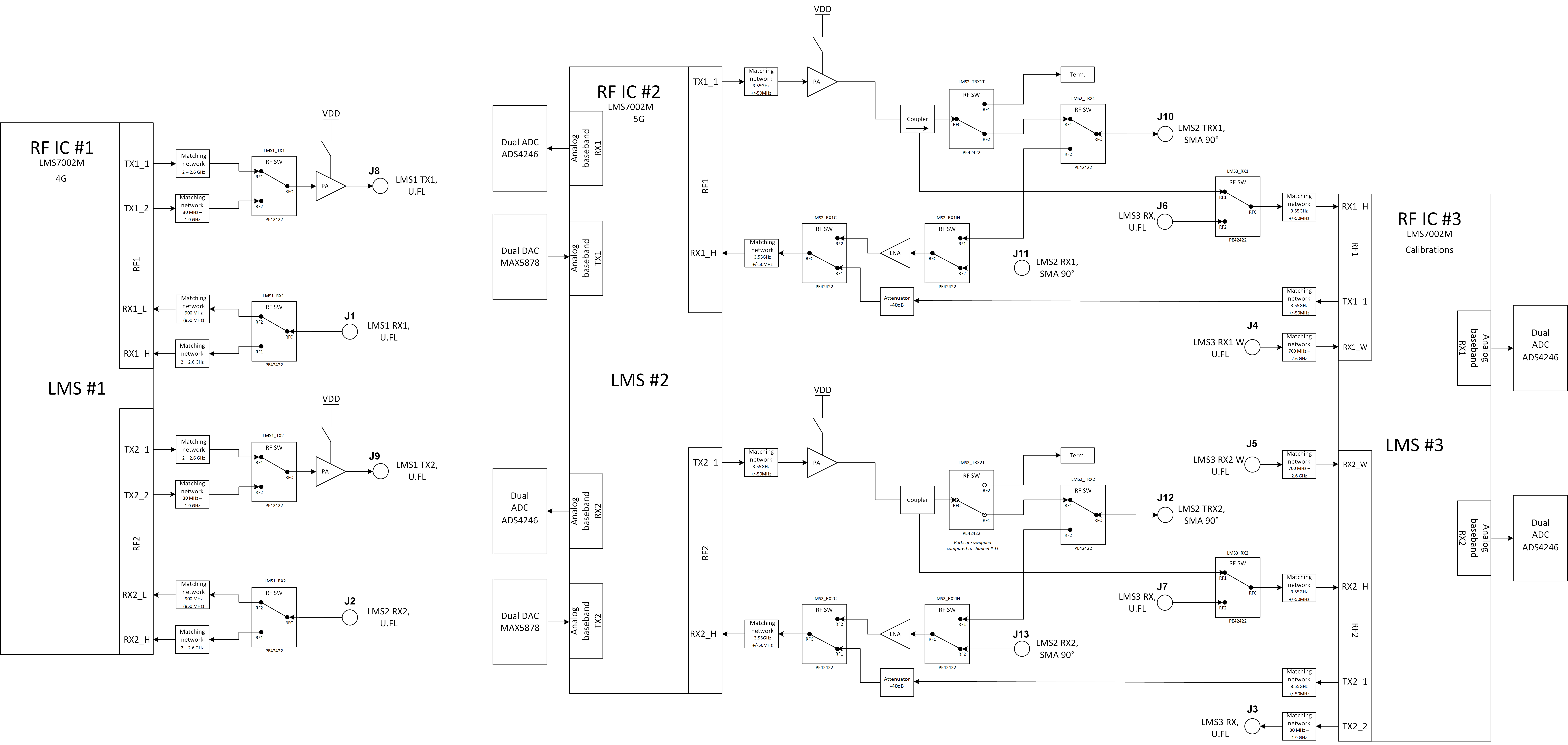
Figure 4. LimeSDR X3 v1.0 RF block diagram
RF transceiver #1 RF path is the simplest. Each TX and RX channel has two frequency-matched channels that can be selected using a 2:1 RF switches. In addition, each TX path has an RF amplifier after band selection. This gives RF transceiver #1 a MIMO system (2x2) with selectable bands in full duplex configuration.
RF transceiver #2 is designed to work in 3.55GHz bands. Each TX and RX channel have fixed frequency matching dedicated for 5G 3.55GHz band. TX paths have PAs with couplers on their outputs. Coupled ports can be fed to RF transceiver #3 RXn_H inputs and can be used for applications like calibrations, DPD etc. Each RX path got LNA. This allows RF transceiver #2 to be configured as a MIMO system (2x2) with selectable bands in full or half duplex configurations.
RF transceiver #3 is dedicated for calibrations. Calibration signals may be fed to RF transceiver #2 RX channels or can receive coupled TX signal from PAs. The RF transceiver #3 also has several TX and RX channels that are routed to the coaxial connectors.
More information about RF transceivers is provided in the next section.
RF transceivers
The LMS7002M is a fully-integrated, multi-band, multi-standard RF transceiver that is highly programmable. It combines Low Noise Amplifiers (RXLNA), TX Power Amplifier Drivers (TXPAD) receiver/transmitter (RX/TX) mixers, RX/TX filters, synthesizers, RX gain control, TX power control, analogue-to-digital and digital-to-analogue converters (ADC/DACs) and has been designed to require very few external components.
There are three LMS7002M field programmable RF transceiver ICs (LMS7002M#1 - IC1, LMS7002M#2 – IC4 and LMS7002M#3 – IC21), interface signals can be acknowledged by corresponding prefixes LMSx_*, where x can be 1, 2 or 3. For example LMS1_* signals belongs to IC1 and LMS2_* belongs to IC4.
In the following manner interface and control signals are described below:
Digital Interface Signals: LMS7002M (IC1) is using data bus LMS1_DIQ1_D[11:0] and LMS1_DIQ2_D[11:0], LMS1_ENABLE_IQSEL1 and LMS1_ENABLE_IQSEL2, LMS1_FCLK1 and LMS1_FCLK2, LMS1_MCLK1 and LMS1_MCLK2 signals to transfer data to/from FPGA. Indexes 1 and 2 indicate transceiver digital data PORT-1 or PORT-2. Any of these ports can be used to transmit or receive data. By default, PORT-1 is selected as receive port and PORT-2 is selected as transmit port. The FCLK# is input clock and MCLK# is output clock for LMS7002M transceiver. TXNRX signals sets ports directions. For LMS7002M interface timing details refer to LMS7002M transceiver datasheet page 12-13 [link]
LMS Control Signals: these signals are used for optional functionality:
LMSx_RXEN, LMSx_TXEN – receiver and transmitter enable/disable signals.
LMS_RESET – LMS7002M reset signal.
SPI Interface: LMS7002M transceiver is configured via 4-wire SPI interface; FPGA_SPI0_SCLK, FPGA_SPI0_MOSI, FPGA_SPI0_LMSx_MISO, FPGA_SPI0_LMSx_SS. The SPI interface is controlled from FPGA.
LMS I2C Interface: LMS EEPROM are connected to this interface.
Interconnections between LMS7002#1 and LMS7002#2 RF transceivers and FPGA, pin names, schematic signal names and FPGA IO standards are listed in Table 3 and Table 4.
Chip pin (IC1) |
Chip reference (IC1) |
Schematic signal name |
FPGA pin |
FPGA I/O standard |
Comments |
|---|---|---|---|---|---|
E5 |
xoscin_tx |
LMS1_TxPLL_CLK |
Connected to clock buffer |
||
AM24 |
xoscin_rx |
LMS1_RxPLL_CLK |
Connected to clock buffer |
||
E27 |
RESET |
LMS1_RESET |
V1 |
2.5V/3.3V |
|
U29 |
TXEN |
LMS1_TXEN |
V6 |
2.5V/3.3V |
|
V34 |
RXEN |
LMS1_RXEN |
AE3 |
2.5V/3.3V |
|
U33 |
CORE_LDO_EN |
LMS1_CORE_LDO_EN |
2.5V/3.3V |
||
AB34 |
MCLK1 |
LMS1_MCLK1 |
AA3 |
2.5V/3.3V |
|
AA33 |
FCLK1 |
LMS1_FCLK1 |
AB2 |
2.5V/3.3V |
|
V32 |
TXNRX1 |
LMS1_TXNRX1 |
AF4 |
2.5V/3.3V |
|
Y32 |
ENABLE_IQSEL1 |
LMS1_EN_IQSEL1 |
AD4 |
2.5V/3.3V |
|
AG31 |
DIQ1_D0 |
LMS1_DIQ1_D0 |
V4 |
2.5V/3.3V |
|
AF30 |
DIQ1_D1 |
LMS1_DIQ1_D1 |
W5 |
2.5V/3.3V |
|
AF34 |
DIQ1_D2 |
LMS1_DIQ1_D2 |
AC6 |
2.5V/3.3V |
|
AE31 |
DIQ1_D3 |
LMS1_DIQ1_D3 |
AB6 |
2.5V/3.3V |
|
AD30 |
DIQ1_D4 |
LMS1_DIQ1_D4 |
W4 |
2.5V/3.3V |
|
AC29 |
DIQ1_D5 |
LMS1_DIQ1_D5 |
AA7 |
2.5V/3.3V |
|
AE33 |
DIQ1_D6 |
LMS1_DIQ1_D6 |
AA5 |
2.5V/3.3V |
|
AD32 |
DIQ1_D7 |
LMS1_DIQ1_D7 |
AB5 |
2.5V/3.3V |
|
AC31 |
DIQ1_D8 |
LMS1_DIQ1_D8 |
AE5 |
2.5V/3.3V |
|
AC33 |
DIQ1_D9 |
LMS1_DIQ1_D9 |
AD5 |
2.5V/3.3V |
|
AB30 |
DIQ1_D10 |
LMS1_DIQ1_D10 |
AC4 |
2.5V/3.3V |
|
AB32 |
DIQ1_D11 |
LMS1_DIQ1_D11 |
AF5 |
2.5V/3.3V |
|
P34 |
MCLK2 |
LMS1_MCLK2 |
AA4 |
2.5V/3.3V |
|
R29 |
FCLK2 |
LMS1_FCLK2 |
AC3 |
2.5V/3.3V |
|
U31 |
TXNRX2 |
LMS1_TXNRX2 |
AF3 |
2.5V/3.3V |
|
R33 |
ENABLE_IQSEL2 |
LMS1_EN_IQSEL2 |
AE2 |
2.5V/3.3V |
|
H30 |
DIQ2_D0 |
LMS1_DIQ2_D0 |
V2 |
2.5V/3.3V |
|
J31 |
DIQ2_D1 |
LMS1_DIQ2_D1 |
V3 |
2.5V/3.3V |
|
K30 |
DIQ2_D2 |
LMS1_DIQ2_D2 |
W1 |
2.5V/3.3V |
|
K32 |
DIQ2_D3 |
LMS1_DIQ2_D3 |
Y1 |
2.5V/3.3V |
|
L31 |
DIQ2_D4 |
LMS1_DIQ2_D4 |
AF2 |
2.5V/3.3V |
|
K34 |
DIQ2_D5 |
LMS1_DIQ2_D5 |
Y3 |
2.5V/3.3V |
|
M30 |
DIQ2_D6 |
LMS1_DIQ2_D6 |
AB1 |
2.5V/3.3V |
|
M32 |
DIQ2_D7 |
LMS1_DIQ2_D7 |
Y2 |
2.5V/3.3V |
|
N31 |
DIQ2_D8 |
LMS1_DIQ2_D8 |
AC1 |
2.5V/3.3V |
|
N33 |
DIQ2_D9 |
LMS1_DIQ2_D9 |
W3 |
2.5V/3.3V |
|
P30 |
DIQ2_D10 |
LMS1_DIQ2_D10 |
AE1 |
2.5V/3.3V |
|
P32 |
DIQ2_D11 |
LMS1_DIQ2_D11 |
AD1 |
2.5V/3.3V |
|
D28 |
SEN |
FPGA_SPI0_LMS1_SS |
W8 |
2.5V/3.3V |
SPI interface |
C29 |
SCLK |
FPGA_SPI0_SCLK |
Y6 |
2.5V/3.3V |
SPI interface |
F30 |
SDIO |
FPGA_SPI0_MOSI |
Y5 |
2.5V/3.3V |
SPI interface |
F28 |
SDO |
FPGA_SPI0_LMS1_MISO |
V8 |
2.5V/3.3V |
SPI interface |
D26 |
SDA |
LMS1_I2C_SDA |
2.5V/3.3V |
Connected to EEPROM |
|
C27 |
SCL |
LMS1_I2C_SCL |
2.5V/3.3V |
Connected to EEPROM |
Chip pin (IC3) |
Chip reference (IC2) |
Schematic signal name |
FPGA pin |
FPGA I/O standard |
Comments |
|---|---|---|---|---|---|
E5 |
xoscin_tx |
LMS2_TxPLL_CLK |
Connected to clock buffer |
||
AM24 |
xoscin_rx |
LMS2_RxPLL_CLK |
Connected to clock buffer |
||
E27 |
RESET |
LMS2_RESET |
V7 |
2.5V/3.3V |
|
U29 |
TXEN |
LMS2_TXEN |
AA8 |
2.5V/3.3V |
|
V34 |
RXEN |
LMS2_RXEN |
Y8 |
2.5V/3.3V |
|
U33 |
CORE_LDO_EN |
LMS2_CORE_LDO_EN |
2.5V/3.3V |
||
D28 |
SEN |
FPGA_SPI0_LMS2_SS |
AA2 |
2.5V/3.3V |
SPI interface |
C29 |
SCLK |
FPGA_SPI0_SCLK |
Y6 |
2.5V/3.3V |
SPI interface |
F30 |
SDIO |
FPGA_SPI0_MOSI |
Y5 |
2.5V/3.3V |
SPI interface |
F28 |
SDO |
FPGA_SPI0_LMS2_MISO |
AB4 |
2.5V/3.3V |
SPI interface |
D26 |
SDA |
LMS2_I2C_SDA |
2.5V/3.3V |
Connected to EEPROM |
|
C27 |
SCL |
LMS2_I2C_SCL |
2.5V/3.3V |
Connected to EEPROM |
Chip pin (IC3) |
Chip reference (IC2) |
Schematic signal name |
FPGA pin |
FPGA I/O standard |
Comments |
|---|---|---|---|---|---|
E5 |
xoscin_tx |
LMS3_TxPLL_CLK |
Connected to clock buffer |
||
AM24 |
xoscin_rx |
LMS3_RxPLL_CLK |
Connected to clock buffer |
||
E27 |
RESET |
LMS3_RESET |
W6 |
2.5V/3.3V |
|
U29 |
TXEN |
LMS3_TXEN |
Y7 |
2.5V/3.3V |
|
V34 |
RXEN |
LMS3_RXEN |
U7 |
2.5V/3.3V |
|
U33 |
CORE_LDO_EN |
LMS3_CORE_LDO_EN |
2.5V/3.3V |
||
D28 |
SEN |
FPGA_SPI0_LMS3_SS |
AC2 |
2.5V/3.3V |
SPI interface |
C29 |
SCLK |
FPGA_SPI0_SCLK |
Y6 |
2.5V/3.3V |
SPI interface |
F30 |
SDIO |
FPGA_SPI0_MOSI |
Y5 |
2.5V/3.3V |
SPI interface |
F28 |
SDO |
FPGA_SPI0_LMS3_MISO |
AD3 |
2.5V/3.3V |
SPI interface |
D26 |
SDA |
LMS3_I2C_SDA |
2.5V/3.3V |
Connected to EEPROM |
|
C27 |
SCL |
LMS3_I2C_SCL |
2.5V/3.3V |
Connected to EEPROM |
Baseband ADCs
There are four Dual-Channel 14-Bit, 160 Msps, analog-to-digital converters (ADS4246 – IC62, IC64, IC66 and IC68). ADC analog inputs are connected to baseband RX outputs of RF transceivers #1 and #2 (IC4 and IC21). Digital output pins are connected to FPGA.
Detailed interface between ADCs and other components including ADC pins, schematic signal names, FPGA pins and FPGA I/O standards is as shown in Table 6, Table 7, Table 8 and Table 9.
Chip pin (IC33) |
Chip reference (IC33) |
Schematic signal name |
FPGA pin |
I/O standard |
|---|---|---|---|---|
41 |
DA0_P/DA1 |
LMS2_BB_ADC1_DA0_P |
B20 |
2.5V |
40 |
DA0_M/DA0 |
LMS2_BB_ADC1_DA0_N |
A20 |
2.5V |
43 |
DA2_P/DA3 |
LMS2_BB_ADC1_DA1_P |
A17 |
2.5V |
42 |
DA2_M/DA2 |
LMS2_BB_ADC1_DA1_N |
A18 |
2.5V |
45 |
DA4_P/DA5 |
LMS2_BB_ADC1_DA2_P |
G17 |
2.5V |
44 |
DA4_M/DA4 |
LMS2_BB_ADC1_DA2_N |
F17 |
2.5V |
47 |
DA6_P/DA7 |
LMS2_BB_ADC1_DA3_P |
B19 |
2.5V |
46 |
DA6_M/DA6 |
LMS2_BB_ADC1_DA3_N |
A19 |
2.5V |
51 |
DA8_P/DA13 |
LMS2_BB_ADC1_DA4_P |
C17 |
2.5V |
50 |
DA8_M/DA12 |
LMS2_BB_ADC1_DA4_N |
B17 |
2.5V |
53 |
DA10_P/DA9 |
LMS2_BB_ADC1_DA5_P |
E16 |
2.5V |
52 |
DA10_M/DA8 |
LMS2_BB_ADC1_DA5_N |
D16 |
2.5V |
55 |
DA12_P/DA11 |
LMS2_BB_ADC1_DA6_P |
B22 |
2.5V |
54 |
DA12_M/DA10 |
LMS2_BB_ADC1_DA6_N |
A22 |
2.5V |
61 |
DB0_P/DB1 |
LMS2_BB_ADC1_DB0_P |
A23 |
2.5V |
60 |
DB0_M/DB0 |
LMS2_BB_ADC1_DB0_N |
A24 |
2.5V |
63 |
DB2_P/DB3 |
LMS2_BB_ADC1_DB1_P |
C26 |
2.5V |
62 |
DB2_M/DB2 |
LMS2_BB_ADC1_DB1_N |
B26 |
2.5V |
3 |
DB4_P/DB5 |
LMS2_BB_ADC1_DB2_P |
F18 |
2.5V |
2 |
DB4_M/DB4 |
LMS2_BB_ADC1_DB2_N |
F19 |
2.5V |
5 |
DB6_P/DB7 |
LMS2_BB_ADC1_DB3_P |
C21 |
2.5V |
4 |
DB6_M/DB6 |
LMS2_BB_ADC1_DB3_N |
B21 |
2.5V |
7 |
DB8_P/DB13 |
LMS2_BB_ADC1_DB4_P |
E21 |
2.5V |
6 |
DB8_M/DB12 |
LMS2_BB_ADC1_DB4_N |
D21 |
2.5V |
9 |
DB10_P/DB9 |
LMS2_BB_ADC1_DB5_P |
C24 |
2.5V |
8 |
DB10_M/DB8 |
LMS2_BB_ADC1_DB5_N |
B24 |
2.5V |
11 |
DB12_P/DB11 |
LMS2_BB_ADC1_DB6_P |
B25 |
2.5V |
10 |
DB12_M/DB10 |
LMS2_BB_ADC1_DB6_N |
A25 |
2.5V |
35 |
CTRL1 |
LMS2_BB_ADC1_CTRL1 |
||
36 |
CTRL2 |
LMS2_BB_ADC1_CTRL2 |
||
34 |
CTRL3 |
LMS2_BB_ADC1_CTRL3 |
||
29 |
INP_A |
LMS2_BB_ADC1_INA_P |
||
30 |
INM_A |
LMS2_BB_ADC1_INA_N |
||
23 |
VCM |
LMS2_BB_ADC1_VCM |
||
57 |
CLKOUTP/CLKOUT |
LMS2_BB_ADC1_CLKOUT_P |
D18 |
2.5V |
56 |
CLKOUTM/UNUSED |
LMS2_BB_ADC1_CLKOUT_N |
C18 |
2.5V |
19 |
INP_B |
LMS2_BB_ADC1_INB_P |
||
20 |
INM_B |
LMS2_BB_ADC1_INB_N |
||
25 |
CLKP |
LMS2_BB_ADC1_CLKC_P |
||
26 |
CLKM |
LMS2_BB_ADC1_CLKC_N |
||
13 |
SCLK |
FPGA_SPI1_SCLK |
M16 |
2.5V |
14 |
SDATA |
FPGA_SPI1_MOSI |
M14 |
2.5V |
64 |
SDOUT |
FPGA_SPI1_MISO_BB_ADC_LS |
E22 |
2.5V |
15 |
SEN |
FPGA_SPI1_LMS2_BB_ADC1_SS |
C22 |
2.5V |
12 |
RESET |
FPGA_LMS2_BB_ADC1_RESET |
D23 |
2.5V |
Chip pin (IC33) |
Chip reference (IC33) |
Schematic signal name |
FPGA pin |
I/O standard |
|---|---|---|---|---|
41 |
DA0_P/DA1 |
LMS2_BB_ADC2_DA0_P |
E25 |
2.5V |
40 |
DA0_M/DA0 |
LMS2_BB_ADC2_DA0_N |
D25 |
2.5V |
43 |
DA2_P/DA3 |
LMS2_BB_ADC2_DA1_P |
K16 |
2.5V |
42 |
DA2_M/DA2 |
LMS2_BB_ADC2_DA1_N |
K17 |
2.5V |
45 |
DA4_P/DA5 |
LMS2_BB_ADC2_DA2_P |
F23 |
2.5V |
44 |
DA4_M/DA4 |
LMS2_BB_ADC2_DA2_N |
E23 |
2.5V |
47 |
DA6_P/DA7 |
LMS2_BB_ADC2_DA3_P |
J19 |
2.5V |
46 |
DA6_M/DA6 |
LMS2_BB_ADC2_DA3_N |
H19 |
2.5V |
51 |
DA8_P/DA13 |
LMS2_BB_ADC2_DA4_P |
G24 |
2.5V |
50 |
DA8_M/DA12 |
LMS2_BB_ADC2_DA4_N |
F24 |
2.5V |
53 |
DA10_P/DA9 |
LMS2_BB_ADC2_DA5_P |
E26 |
2.5V |
52 |
DA10_M/DA8 |
LMS2_BB_ADC2_DA5_N |
D26 |
2.5V |
55 |
DA12_P/DA11 |
LMS2_BB_ADC2_DA6_P |
G25 |
2.5V |
54 |
DA12_M/DA10 |
LMS2_BB_ADC2_DA6_N |
F25 |
2.5V |
61 |
DB0_P/DB1 |
LMS2_BB_ADC2_DB0_P |
H26 |
2.5V |
60 |
DB0_M/DB0 |
LMS2_BB_ADC2_DB0_N |
G26 |
2.5V |
63 |
DB2_P/DB3 |
LMS2_BB_ADC2_DB1_P |
J25 |
2.5V |
62 |
DB2_M/DB2 |
LMS2_BB_ADC2_DB1_N |
J26 |
2.5V |
3 |
DB4_P/DB5 |
LMS2_BB_ADC2_DB2_P |
J24 |
2.5V |
2 |
DB4_M/DB4 |
LMS2_BB_ADC2_DB2_N |
H24 |
2.5V |
5 |
DB6_P/DB7 |
LMS2_BB_ADC2_DB3_P |
J18 |
2.5V |
4 |
DB6_M/DB6 |
LMS2_BB_ADC2_DB3_N |
H18 |
2.5V |
7 |
DB8_P/DB13 |
LMS2_BB_ADC2_DB4_P |
K20 |
2.5V |
6 |
DB8_M/DB12 |
LMS2_BB_ADC2_DB4_N |
J20 |
2.5V |
9 |
DB10_P/DB9 |
LMS2_BB_ADC2_DB5_P |
G22 |
2.5V |
8 |
DB10_M/DB8 |
LMS2_BB_ADC2_DB5_N |
F22 |
2.5V |
11 |
DB12_P/DB11 |
LMS2_BB_ADC2_DB6_P |
L17 |
2.5V |
10 |
DB12_M/DB10 |
LMS2_BB_ADC2_DB6_N |
L18 |
2.5V |
35 |
CTRL1 |
LMS2_BB_ADC2_CTRL1 |
||
36 |
CTRL2 |
LMS2_BB_ADC2_CTRL2 |
||
34 |
CTRL3 |
LMS2_BB_ADC2_CTRL3 |
||
29 |
INP_A |
LMS2_BB_ADC2_INA_P |
||
30 |
INM_A |
LMS2_BB_ADC2_INA_N |
||
23 |
VCM |
LMS2_BB_ADC2_VCM |
||
57 |
CLKOUTP/CLKOUT |
LMS2_BB_ADC2_CLKOUT_P |
K21 |
2.5V |
56 |
CLKOUTM/UNUSED |
LMS2_BB_ADC2_CLKOUT_N |
J21 |
2.5V |
19 |
INP_B |
LMS2_BB_ADC2_INB_P |
||
20 |
INM_B |
LMS2_BB_ADC2_INB_N |
||
25 |
CLKP |
LMS2_BB_ADC2_CLKC_P |
||
26 |
CLKM |
LMS2_BB_ADC2_CLKC_N |
||
13 |
SCLK |
FPGA_SPI1_SCLK |
M16 |
2.5V |
14 |
SDATA |
FPGA_SPI1_MOSI |
M14 |
2.5V |
64 |
SDOUT |
FPGA_SPI1_MISO_BB_ADC_LS |
E22 |
2.5V |
15 |
SEN |
FPGA_SPI1_LMS2_BB_ADC2_SS |
K22 |
2.5V |
12 |
RESET |
FPGA_LMS2_BB_ADC2_RESET |
K23 |
2.5V |
Chip pin (IC33) |
Chip reference (IC33) |
Schematic signal name |
FPGA pin |
I/O standard |
|---|---|---|---|---|
41 |
DA0_P/DA1 |
LMS3_BB_ADC1_DA0_P |
AD25 |
2.5V |
40 |
DA0_M/DA0 |
LMS3_BB_ADC1_DA0_N |
AD26 |
2.5V |
43 |
DA2_P/DA3 |
LMS3_BB_ADC1_DA1_P |
AC22 |
2.5V |
42 |
DA2_M/DA2 |
LMS3_BB_ADC1_DA1_N |
AC23 |
2.5V |
45 |
DA4_P/DA5 |
LMS3_BB_ADC1_DA2_P |
AE25 |
2.5V |
44 |
DA4_M/DA4 |
LMS3_BB_ADC1_DA2_N |
AE26 |
2.5V |
47 |
DA6_P/DA7 |
LMS3_BB_ADC1_DA3_P |
AF24 |
2.5V |
46 |
DA6_M/DA6 |
LMS3_BB_ADC1_DA3_N |
AF25 |
2.5V |
51 |
DA8_P/DA13 |
LMS3_BB_ADC1_DA4_P |
AF19 |
2.5V |
50 |
DA8_M/DA12 |
LMS3_BB_ADC1_DA4_N |
AF20 |
2.5V |
53 |
DA10_P/DA9 |
LMS3_BB_ADC1_DA5_P |
AE18 |
2.5V |
52 |
DA10_M/DA8 |
LMS3_BB_ADC1_DA5_N |
AF18 |
2.5V |
55 |
DA12_P/DA11 |
LMS3_BB_ADC1_DA6_P |
AE17 |
2.5V |
54 |
DA12_M/DA10 |
LMS3_BB_ADC1_DA6_N |
AF17 |
2.5V |
61 |
DB0_P/DB1 |
LMS3_BB_ADC1_DB0_P |
AC17 |
2.5V |
60 |
DB0_M/DB0 |
LMS3_BB_ADC1_DB0_N |
AD17 |
2.5V |
63 |
DB2_P/DB3 |
LMS3_BB_ADC1_DB1_P |
Y16 |
2.5V |
62 |
DB2_M/DB2 |
LMS3_BB_ADC1_DB1_N |
Y17 |
2.5V |
3 |
DB4_P/DB5 |
LMS3_BB_ADC1_DB2_P |
Y18 |
2.5V |
2 |
DB4_M/DB4 |
LMS3_BB_ADC1_DB2_N |
AA18 |
2.5V |
5 |
DB6_P/DB7 |
LMS3_BB_ADC1_DB3_P |
AD20 |
2.5V |
4 |
DB6_M/DB6 |
LMS3_BB_ADC1_DB3_N |
AE20 |
2.5V |
7 |
DB8_P/DB13 |
LMS3_BB_ADC1_DB4_P |
AD21 |
2.5V |
6 |
DB8_M/DB12 |
LMS3_BB_ADC1_DB4_N |
AE21 |
2.5V |
9 |
DB10_P/DB9 |
LMS3_BB_ADC1_DB5_P |
AE22 |
2.5V |
8 |
DB10_M/DB8 |
LMS3_BB_ADC1_DB5_N |
AF22 |
2.5V |
11 |
DB12_P/DB11 |
LMS3_BB_ADC1_DB6_P |
AE23 |
2.5V |
10 |
DB12_M/DB10 |
LMS3_BB_ADC1_DB6_N |
AF23 |
2.5V |
35 |
CTRL1 |
LMS3_BB_ADC1_CTRL1 |
||
36 |
CTRL2 |
LMS3_BB_ADC1_CTRL2 |
||
34 |
CTRL3 |
LMS3_BB_ADC1_CTRL3 |
||
29 |
INP_A |
LMS3_BB_ADC1_INA_P |
||
30 |
INM_A |
LMS3_BB_ADC1_INA_N |
||
23 |
VCM |
LMS3_BB_ADC1_VCM |
||
57 |
CLKOUTP/CLKOUT |
LMS3_BB_ADC1_CLKOUT_P |
AA20 |
2.5V |
56 |
CLKOUTM/UNUSED |
LMS3_BB_ADC1_CLKOUT_N |
AB20 |
2.5V |
19 |
INP_B |
LMS3_BB_ADC1_INB_P |
||
20 |
INM_B |
LMS3_BB_ADC1_INB_N |
||
25 |
CLKP |
LMS3_BB_ADC1_CLKC_P |
||
26 |
CLKM |
LMS3_BB_ADC1_CLKC_N |
||
13 |
SCLK |
FPGA_SPI1_SCLK |
M16 |
2.5V |
14 |
SDATA |
FPGA_SPI1_MOSI |
M14 |
2.5V |
64 |
SDOUT |
FPGA_SPI1_MISO_BB_ADC_LS |
E22 |
2.5V |
15 |
SEN |
FPGA_SPI1_LMS3_BB_ADC1_SS |
F20 |
2.5V |
12 |
RESET |
FPGA_LMS3_BB_ADC1_RESET |
D24 |
2.5V |
Chip pin (IC33) |
Chip reference (IC33) |
Schematic signal name |
FPGA pin |
I/O standard |
|---|---|---|---|---|
41 |
DA0_P/DA1 |
LMS3_BB_ADC2_DA0_P |
T14 |
2.5V |
40 |
DA0_M/DA0 |
LMS3_BB_ADC2_DA0_N |
T15 |
2.5V |
43 |
DA2_P/DA3 |
LMS3_BB_ADC2_DA1_P |
T17 |
2.5V |
42 |
DA2_M/DA2 |
LMS3_BB_ADC2_DA1_N |
T18 |
2.5V |
45 |
DA4_P/DA5 |
LMS3_BB_ADC2_DA2_P |
V23 |
2.5V |
44 |
DA4_M/DA4 |
LMS3_BB_ADC2_DA2_N |
W23 |
2.5V |
47 |
DA6_P/DA7 |
LMS3_BB_ADC2_DA3_P |
T19 |
2.5V |
46 |
DA6_M/DA6 |
LMS3_BB_ADC2_DA3_N |
U19 |
2.5V |
51 |
DA8_P/DA13 |
LMS3_BB_ADC2_DA4_P |
AA22 |
2.5V |
50 |
DA8_M/DA12 |
LMS3_BB_ADC2_DA4_N |
AA23 |
2.5V |
53 |
DA10_P/DA9 |
LMS3_BB_ADC2_DA5_P |
U25 |
2.5V |
52 |
DA10_M/DA8 |
LMS3_BB_ADC2_DA5_N |
U26 |
2.5V |
55 |
DA12_P/DA11 |
LMS3_BB_ADC2_DA6_P |
V26 |
2.5V |
54 |
DA12_M/DA10 |
LMS3_BB_ADC2_DA6_N |
W26 |
2.5V |
61 |
DB0_P/DB1 |
LMS3_BB_ADC2_DB0_P |
AB26 |
2.5V |
60 |
DB0_M/DB0 |
LMS3_BB_ADC2_DB0_N |
AC26 |
2.5V |
63 |
DB2_P/DB3 |
LMS3_BB_ADC2_DB1_P |
AA24 |
2.5V |
62 |
DB2_M/DB2 |
LMS3_BB_ADC2_DB1_N |
AB25 |
2.5V |
3 |
DB4_P/DB5 |
LMS3_BB_ADC2_DB2_P |
W20 |
2.5V |
2 |
DB4_M/DB4 |
LMS3_BB_ADC2_DB2_N |
Y20 |
2.5V |
5 |
DB6_P/DB7 |
LMS3_BB_ADC2_DB3_P |
AB24 |
2.5V |
4 |
DB6_M/DB6 |
LMS3_BB_ADC2_DB3_N |
AC24 |
2.5V |
7 |
DB8_P/DB13 |
LMS3_BB_ADC2_DB4_P |
V19 |
2.5V |
6 |
DB8_M/DB12 |
LMS3_BB_ADC2_DB4_N |
W19 |
2.5V |
9 |
DB10_P/DB9 |
LMS3_BB_ADC2_DB5_P |
Y25 |
2.5V |
8 |
DB10_M/DB8 |
LMS3_BB_ADC2_DB5_N |
AA25 |
2.5V |
11 |
DB12_P/DB11 |
LMS3_BB_ADC2_DB6_P |
W25 |
2.5V |
10 |
DB12_M/DB10 |
LMS3_BB_ADC2_DB6_N |
Y26 |
2.5V |
35 |
CTRL1 |
LMS3_BB_ADC2_CTRL1 |
||
36 |
CTRL2 |
LMS3_BB_ADC2_CTRL2 |
||
34 |
CTRL3 |
LMS3_BB_ADC2_CTRL3 |
||
29 |
INP_A |
LMS3_BB_ADC2_INA_P |
||
30 |
INM_A |
LMS3_BB_ADC2_INA_N |
||
23 |
VCM |
LMS3_BB_ADC2_VCM |
||
57 |
CLKOUTP/CLKOUT |
LMS3_BB_ADC2_CLKOUT_P |
U22 |
2.5V |
56 |
CLKOUTM/UNUSED |
LMS3_BB_ADC2_CLKOUT_N |
V22 |
2.5V |
19 |
INP_B |
LMS3_BB_ADC2_INB_P |
||
20 |
INM_B |
LMS3_BB_ADC2_INB_N |
||
25 |
CLKP |
LMS3_BB_ADC2_CLKC_P |
||
26 |
CLKM |
LMS3_BB_ADC2_CLKC_N |
||
13 |
SCLK |
FPGA_SPI1_SCLK |
M16 |
2.5V |
14 |
SDATA |
FPGA_SPI1_MOSI |
M14 |
2.5V |
64 |
SDOUT |
FPGA_SPI1_MISO_BB_ADC_LS |
E22 |
2.5V |
15 |
SEN |
FPGA_SPI1_LMS3_BB_ADC2_SS |
E20 |
2.5V |
12 |
RESET |
FPGA_LMS3_BB_ADC2_RESET |
D20 |
2.5V |
Baseband DACs
There are two Dual-Channel 16-Bit, 250Msps, digital-to-analog converters (MAX5878 – IC60, and IC61). DAC analog outputs are connected to baseband TX inputs of RF transceivers #2 (IC20). Digital input pins are connected to FPGA.
Detailed interface between DACs and other components including DAC pins, schematic signal names, FPGA pins and FPGA I/O standards is as shown in Table 10 and Table 11.
Chip pin (IC33) |
Chip reference (IC33) |
Schematic signal name |
FPGA pin |
I/O standard |
|---|---|---|---|---|
9 |
B0N |
LMS2_BB_DAC1_B0_N |
M1 |
2.5V |
8 |
B0P |
LMS2_BB_DAC1_B0_P |
N1 |
2.5V |
7 |
B1N |
LMS2_BB_DAC1_B1_N |
R6 |
2.5V |
6 |
B1P |
LMS2_BB_DAC1_B1_P |
R7 |
2.5V |
5 |
B2N |
LMS2_BB_DAC1_B2_N |
L7 |
2.5V |
4 |
B2P |
LMS2_BB_DAC1_B2_P |
M7 |
2.5V |
3 |
B3N |
LMS2_BB_DAC1_B3_N |
T7 |
2.5V |
2 |
B3P |
LMS2_BB_DAC1_B3_P |
T8 |
2.5V |
1 |
B4N |
LMS2_BB_DAC1_B4_N |
P8 |
2.5V |
68 |
B4P |
LMS2_BB_DAC1_B4_P |
R8 |
2.5V |
67 |
B5N |
LMS2_BB_DAC1_B5_N |
U5 |
2.5V |
66 |
B5P |
LMS2_BB_DAC1_B5_P |
U6 |
2.5V |
65 |
B6N |
LMS2_BB_DAC1_B6_N |
P5 |
2.5V |
64 |
B6P |
LMS2_BB_DAC1_B6_P |
P6 |
2.5V |
63 |
B7N |
LMS2_BB_DAC1_B7_N |
R5 |
2.5V |
62 |
B7P |
LMS2_BB_DAC1_B7_P |
T5 |
2.5V |
60 |
B8N |
LMS2_BB_DAC1_B8_N |
U1 |
2.5V |
59 |
B8P |
LMS2_BB_DAC1_B8_P |
U2 |
2.5V |
58 |
B9N |
LMS2_BB_DAC1_B9_N |
R2 |
2.5V |
57 |
B9P |
LMS2_BB_DAC1_B9_P |
T2 |
2.5V |
56 |
B10N |
LMS2_BB_DAC1_B10_N |
P1 |
2.5V |
55 |
B10P |
LMS2_BB_DAC1_B10_P |
R1 |
2.5V |
54 |
B11N |
LMS2_BB_DAC1_B11_N |
T3 |
2.5V |
53 |
B11P |
LMS2_BB_DAC1_B11_P |
T4 |
2.5V |
52 |
B12N |
LMS2_BB_DAC1_B12_N |
L4 |
2.5V |
51 |
B12P |
LMS2_BB_DAC1_B12_P |
M4 |
2.5V |
50 |
B13N |
LMS2_BB_DAC1_B13_N |
J3 |
2.5V |
49 |
B13P |
LMS2_BB_DAC1_B13_P |
K3 |
2.5V |
48 |
B14N |
LMS2_BB_DAC1_B14_N |
J1 |
2.5V |
47 |
B14P |
LMS2_BB_DAC1_B14_P |
K1 |
2.5V |
46 |
B15N |
LMS2_BB_DAC1_B15_N |
H1 |
2.5V |
45 |
B15P |
LMS2_BB_DAC1_B15_P |
H2 |
2.5V |
37 |
CLKN |
LMS2_BB_DAC1_CLK_N |
L2 |
2.5V |
38 |
CLKP |
LMS2_BB_DAC1_CLK_P |
M2 |
2.5V |
43 |
SELIQP |
LMS2_BB_DAC1_SELIQ_P |
M6 |
2.5V |
44 |
SELIQN |
LMS2_BB_DAC1_SELIQ_N |
M5 |
2.5V |
40 |
PD |
LMS2_BB_DAC1_PD |
M26 |
3.3V |
Chip pin (IC33) |
Chip reference (IC33) |
Schematic signal name |
FPGA pin |
I/O standard |
|---|---|---|---|---|
9 |
B0N |
LMS2_BB_DAC2_B0_N |
D6 |
2.5V |
8 |
B0P |
LMS2_BB_DAC2_B0_P |
E6 |
2.5V |
7 |
B1N |
LMS2_BB_DAC2_B1_N |
G7 |
2.5V |
6 |
B1P |
LMS2_BB_DAC2_B1_P |
H7 |
2.5V |
5 |
B2N |
LMS2_BB_DAC2_B2_N |
E3 |
2.5V |
4 |
B2P |
LMS2_BB_DAC2_B2_P |
F3 |
2.5V |
3 |
B3N |
LMS2_BB_DAC2_B3_N |
K6 |
2.5V |
2 |
B3P |
LMS2_BB_DAC2_B3_P |
K7 |
2.5V |
1 |
B4N |
LMS2_BB_DAC2_B4_N |
H4 |
2.5V |
68 |
B4P |
LMS2_BB_DAC2_B4_P |
J4 |
2.5V |
67 |
B5N |
LMS2_BB_DAC2_B5_N |
E2 |
2.5V |
66 |
B5P |
LMS2_BB_DAC2_B5_P |
F2 |
2.5V |
65 |
B6N |
LMS2_BB_DAC2_B6_N |
D1 |
2.5V |
64 |
B6P |
LMS2_BB_DAC2_B6_P |
E1 |
2.5V |
63 |
B7N |
LMS2_BB_DAC2_B7_N |
B1 |
2.5V |
62 |
B7P |
LMS2_BB_DAC2_B7_P |
C1 |
2.5V |
60 |
B8N |
LMS2_BB_DAC2_B8_N |
C3 |
2.5V |
59 |
B8P |
LMS2_BB_DAC2_B8_P |
D3 |
2.5V |
58 |
B9N |
LMS2_BB_DAC2_B9_N |
A4 |
2.5V |
57 |
B9P |
LMS2_BB_DAC2_B9_P |
B4 |
2.5V |
56 |
B10N |
LMS2_BB_DAC2_B10_N |
A2 |
2.5V |
55 |
B10P |
LMS2_BB_DAC2_B10_P |
A3 |
2.5V |
54 |
B11N |
LMS2_BB_DAC2_B11_N |
A5 |
2.5V |
53 |
B11P |
LMS2_BB_DAC2_B11_P |
B5 |
2.5V |
52 |
B12N |
LMS2_BB_DAC2_B12_N |
G6 |
2.5V |
51 |
B12P |
LMS2_BB_DAC2_B12_P |
H6 |
2.5V |
50 |
B13N |
LMS2_BB_DAC2_B13_N |
F7 |
2.5V |
49 |
B13P |
LMS2_BB_DAC2_B13_P |
F8 |
2.5V |
48 |
B14N |
LMS2_BB_DAC2_B14_N |
G9 |
2.5V |
47 |
B14P |
LMS2_BB_DAC2_B14_P |
H9 |
2.5V |
46 |
B15N |
LMS2_BB_DAC2_B15_N |
G8 |
2.5V |
45 |
B15P |
LMS2_BB_DAC2_B15_P |
H8 |
2.5V |
37 |
CLKN |
LMS2_BB_DAC2_CLK_N |
D5 |
2.5V |
38 |
CLKP |
LMS2_BB_DAC2_CLK_P |
E5 |
2.5V |
43 |
SELIQP |
LMS2_BB_DAC2_SELIQ_P |
L8 |
2.5V |
44 |
SELIQN |
LMS2_BB_DAC2_SELIQ_N |
K8 |
2.5V |
40 |
PD |
LMS2_BB_DAC2_PD |
N24 |
3.3V |
GNSS module
GNSS module LYNQ N20B (IC58) can be used not only for positioning applications but for frequency measuring and tuning applications also (e. g. GPS disciplined oscillator - GPSDO). It provides 1PPS time synchronization pulse which is connected to FPGA for further processing. Connection to FPGA is as shown in Table 12.
Chip pin (IC14) |
Chip reference (IC14) |
Schematic signal name |
FPGA pin |
I/O standard |
|---|---|---|---|---|
3 |
TIMEPULSE |
GNSS_TPULSE |
L20 |
3.3V |
20 |
UART_TX |
GNSS_UART_TX |
L24 |
3.3V |
21 |
UART_RX |
GNSS_UART_RX |
L25 |
3.3V |
External GNSS antenna SMA connector (J21) supports active antennas (3.3V).
PMOD connectors
Two ten pin 0.1” pitch right angle PMOD connectors (J15, J19) are connected to the FPGA. Pinout description, dedicated FPGA pins and FPGA I/O standard is shown in Table 13 and Table 14.
Connector pin |
Schematic signal name |
FPGA pin |
I/O standard |
Comment |
|---|---|---|---|---|
1 |
PMOD_A_PIN1 |
R25 |
3.3V |
|
2 |
PMOD_A_PIN2 |
P23 |
3.3V |
|
3 |
PMOD_A_PIN3 |
P21 |
3.3V |
|
4 |
PMOD_A_PIN4 |
P19 |
3.3V |
|
7 |
PMOD_A_PIN7 |
R20 |
3.3V |
|
8 |
PMOD_A_PIN8 |
R21 |
3.3V |
|
9 |
PMOD_A_PIN9 |
P15 |
3.3V |
|
10 |
PMOD_A_PIN10 |
P16 |
3.3V |
|
5,11 |
GND |
|||
6,12 |
VCC |
3.3V (default) or 5V selectable power rail. |
Connector pin |
Schematic signal name |
FPGA pin |
I/O standard |
Comment |
|---|---|---|---|---|
1 |
PMOD_B_PIN1 |
L23 |
3.3V |
|
2 |
PMOD_B_PIN2 |
M24 |
3.3V |
|
3 |
PMOD_B_PIN3 |
M22 |
3.3V |
|
4 |
PMOD_B_PIN4 |
N22 |
3.3V |
|
7 |
PMOD_B_PIN7 |
N19 |
3.3V |
|
8 |
PMOD_B_PIN8 |
P24 |
3.3V |
|
9 |
PMOD_B_PIN9 |
P25 |
3.3V |
|
10 |
PMOD_B_PIN10 |
N23 |
3.3V |
|
5,11 |
GND |
|||
6,12 |
VCC |
3.3V (default) or 5V selectable power rail. |
Pins 6 and 12 of each PMOD connector provides output voltage of 3.3V (default) or 5V. To provide 5V instead of 3.3V remove R181 and solder R182 resistor for PMOD#A; remove R203 and solder R204 resistor for PMOD#B as shown in Figure 5.
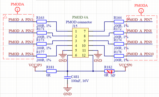
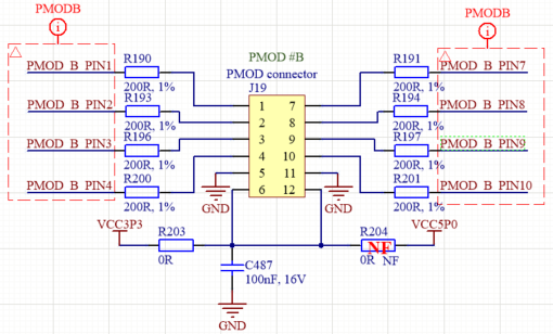
Figure 5. PMOD connectors
Indication LEDs
LimeSDR X3 board features six dual color (red and green (RG)) indication LEDs. Most of LEDs are connected to FPGA and their function may be programmed according to the user requirements. Default function of LEDs and related information is listed in Table 15.
Board Reference |
Schematic name |
Board label |
FPGA pin |
Description |
|---|---|---|---|---|
LED1 |
FPGA_LED1_R |
LED1 |
U17 |
|
FPGA_LED1_G |
T20 |
|||
LED2 |
FPGA_LED2_R |
LED2 |
V17 |
|
FPGA_LED2_G |
U16 |
|||
LED3 |
FPGA_LED3_R |
LED3 |
V16 |
|
FPGA_LED3_G |
U15 |
|||
LED4 |
FPGA_LED4_R |
LED4 |
V14 |
|
FPGA_LED4_G |
U14 |
|||
LED5 |
LED5 VCC3P3 |
Green LED indicates VCC3P3 power rail presence. Red LED is unused. |
||
LED6 |
FPGA_DONE |
LED6 FPGA_DONE LED |
W10 |
Green LED indicates board ready to use. Red LED indicates FPGA initialization failure. |
DIP Switches
Four bit DIP switch SW1 is connected to FPGA and may be used to implement additional functionality which requires input control. Each switch line has external pull up resistor. When switch is in position “On”, it pulls the line down to logic ‘0’ level.
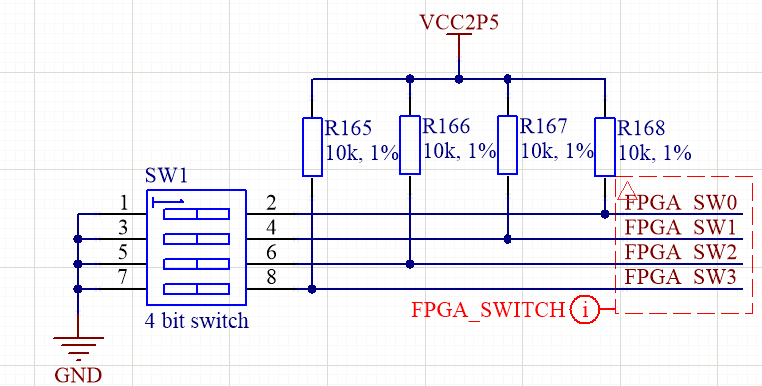
Figure 6. LimeSDR X3 four poles slide switch
Switch and FPGA interconnection is as shown in Table 16.
Switch pole |
Schematic signal name |
FPGA pin (IC29) |
I/O standard |
|---|---|---|---|
1 |
FPGA_SW0 |
K5 |
2.5V |
2 |
FPGA_SW1 |
L5 |
2.5V |
3 |
FPGA_SW2 |
G1 |
2.5V |
4 |
FPGA_SW3 |
G2 |
2.5V |
Temperature sensor and fan control
LimeSDR X3 board has integrated temperature sensor which can be used to monitor board temperature through I2C interface.
Sensor has over temperature shutdown (OS) output connected to FPGA which can be used to take actions to reduce board temperature when it rises above set limits. For example, fan will be turned on if board will heat up to 45°C and FAN will be turned off if board will cool down to 35°C as shown in Figure 7. These values can be modified.
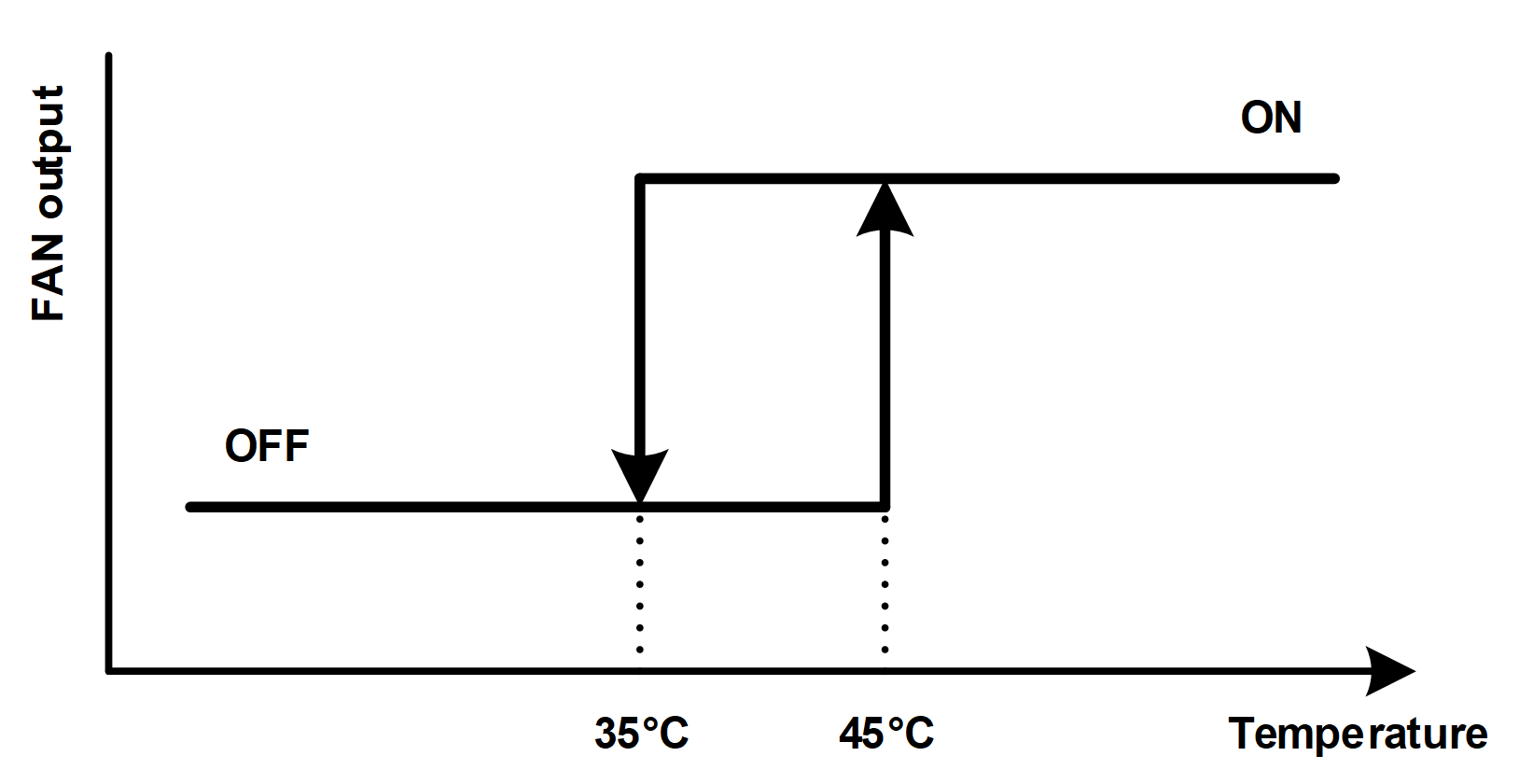
Figure 7. FAN control temperature hysteresis
Schematic signal name |
FPGA pin |
I/O standard |
Comment |
|---|---|---|---|
FPGA_I2C_SCL |
N16 |
3.3V |
Serial Clock |
FPGA_I2C_SDA |
N17 |
3.3V |
Data |
LM75_OS |
U24 |
2.5V |
Overtemperature shutdown output (FPGA input) |
FAN_CTRL |
U4 |
2.5V |
Fan control output |
Fan voltage can be selected between 3.3V, 5V (default) and 12V via R186, R187 and R188 respectively as shown in Figure 8. Up to three fans can be connected to connectors: J18 (FPGA), J16 (RF) and J17 (spare).
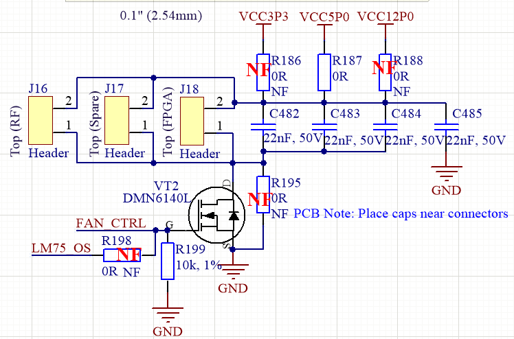
Figure 8. Fan control circuit and voltage selection resistors
Clock Distribution
LimeSDR X3 board has onboard VCOCXO U7475LF (XO3 – 30.72 MHz) (default), VCTCXO E6245LF, E5280LF (XO4, XO5 - 30.7 MHz), ASVTX-12-A-38.400MHZ-H10-T (XO7 – 38.4 MHz) and RTX5032A (XO6 – 40 MHz) oscillators that can be used as source for clock buffer LMK00101 and clock generator CDCM6208. By default XO3 is connected to the clock buffer primary reference input. All these XOs can be tuned by 16-bit DAC (IC77), phase detector (IC76) or by FPGA using GPIO in PWM mode.
Using header J30 connector is possible to connect external reference clock and PPS signal from another board. Header J31 can be used to feed reference clock and PPS signal to another board. Headers J30 and J31 can be used to synchronize several boards by daisy chaining each other.
Using J27 coaxial connector it is possible to feed external reference clock.
For Frequency and phase synchronization over network implementation (Precision Time Protocol (White Rabbit)) there is some dedicated hardware on the board: 25 MHz VCTXCO (XO1) and 20 MHz VCXO (XO2), clock generator CDCM61004 (IC71), 16 bit XO DACs (IC70, IC73) and SFP cage (J24).
There is 100 MHz crystal oscillator (XO4) connected to FPGA.
Clock distribution block diagram is as shown in Figure 9.
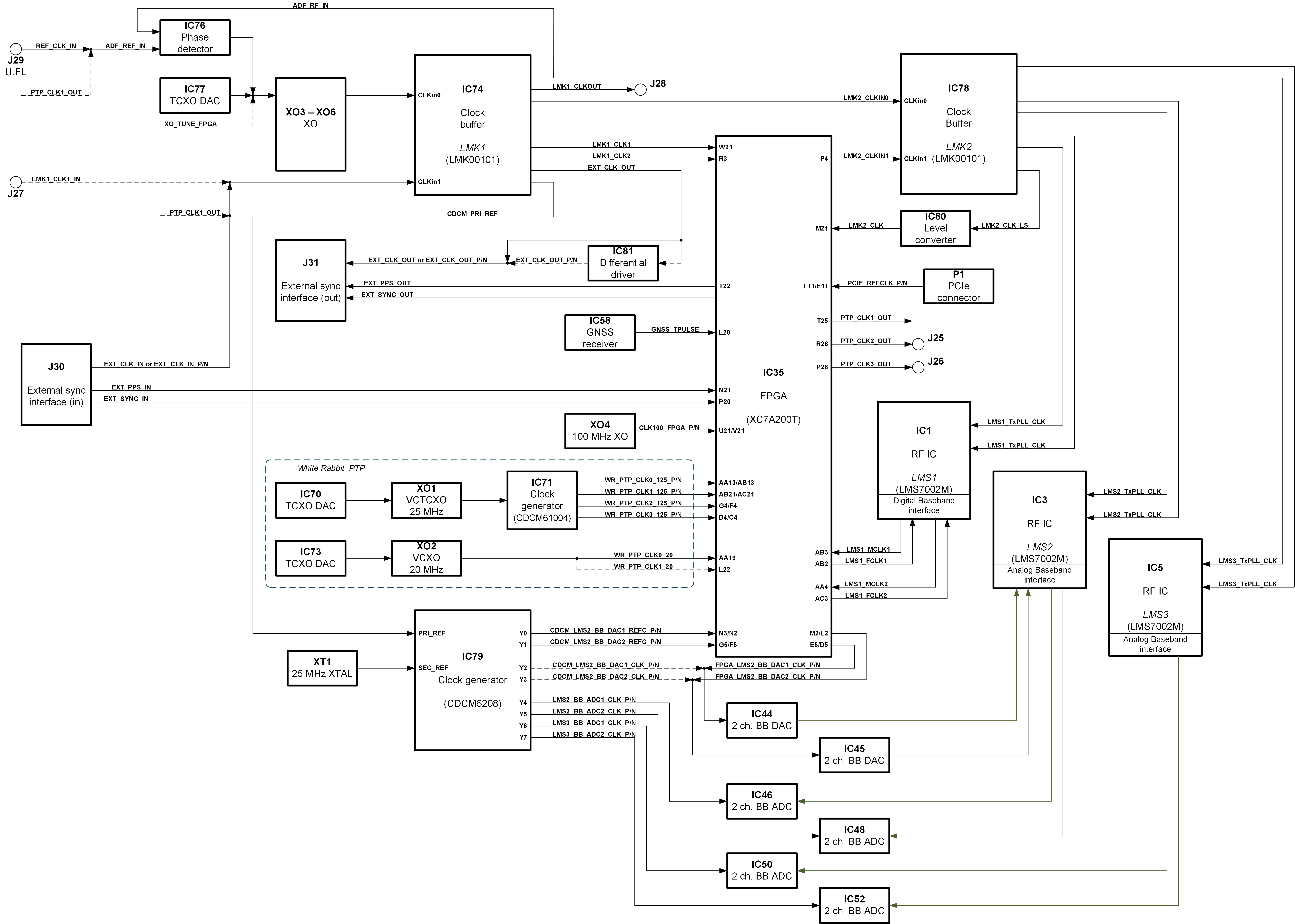
Figure 9. LimeSDR X3 board clock distribution block diagram
Source |
Schematic signal name |
I/O standard |
FPGA pin |
Description |
|---|---|---|---|---|
Clock buffer (LMK1 –IC74) |
LMK1_CLK1 |
2.5V |
W21 |
|
LMK1_CLK2 |
2.5V |
R3 |
||
LMK2_CLKIN0 |
2.5V |
Connected to LMK2 |
||
ADF_RF_IN |
2.5V |
Connected to ADF4002 |
||
CDCM_PRI_REF |
2.5V |
Connected to CDCM6208 |
||
LMK1_CLKOUT |
3.3V |
Connected to J28 |
||
EXT_CLK_OUT |
3.3V |
Connected to J31 |
||
Clock buffer (LMK2 –IC78) |
LMS1_TxPLL_CLK |
1.8V |
Connected to LMS1 |
|
LMS1_RxPLL_CLK |
1.8V |
Connected to LMS1 |
||
LMS2_TxPLL_CLK |
1.8V |
Connected to LMS2 |
||
LMS2_RxPLL_CLK |
1.8V |
Connected to LMS2 |
||
LMS3_TxPLL_CLK |
1.8V |
Connected to LMS3 |
||
LMS3_RxPLL_CLK |
1.8V |
Connected to LMS3 |
||
RF transceiver #1 (IC1) |
LMS1_MCLK1 |
2.5V/3.3V |
AA3 |
|
LMS1_FCLK1 |
2.5V/3.3V |
AB2 |
||
LMS1_MCLK2 |
2.5V/3.3V |
AA4 |
||
LMS1_FCLK2 |
2.5V/3.3V |
AC3 |
||
GNSS module IC14 |
GNSS_TPULSE |
3.3V |
L20 |
1PPS time pulse output |
Power Distribution
LimeSDR X3 board by default must be powered from 12V 6 pin PCIe power connector (J36) due to high power consumption. An alternative 12V supply connection is possible from the PCI connector (disabled by default) if a power consumption of less than 25W is guaranteed.
Header J34 (0.2” pitch) and J35 (0.1” pitch) can be used for powering external 12V devices.
LimeSDR X3 board power distribution diagram is as shown in Figure 10.
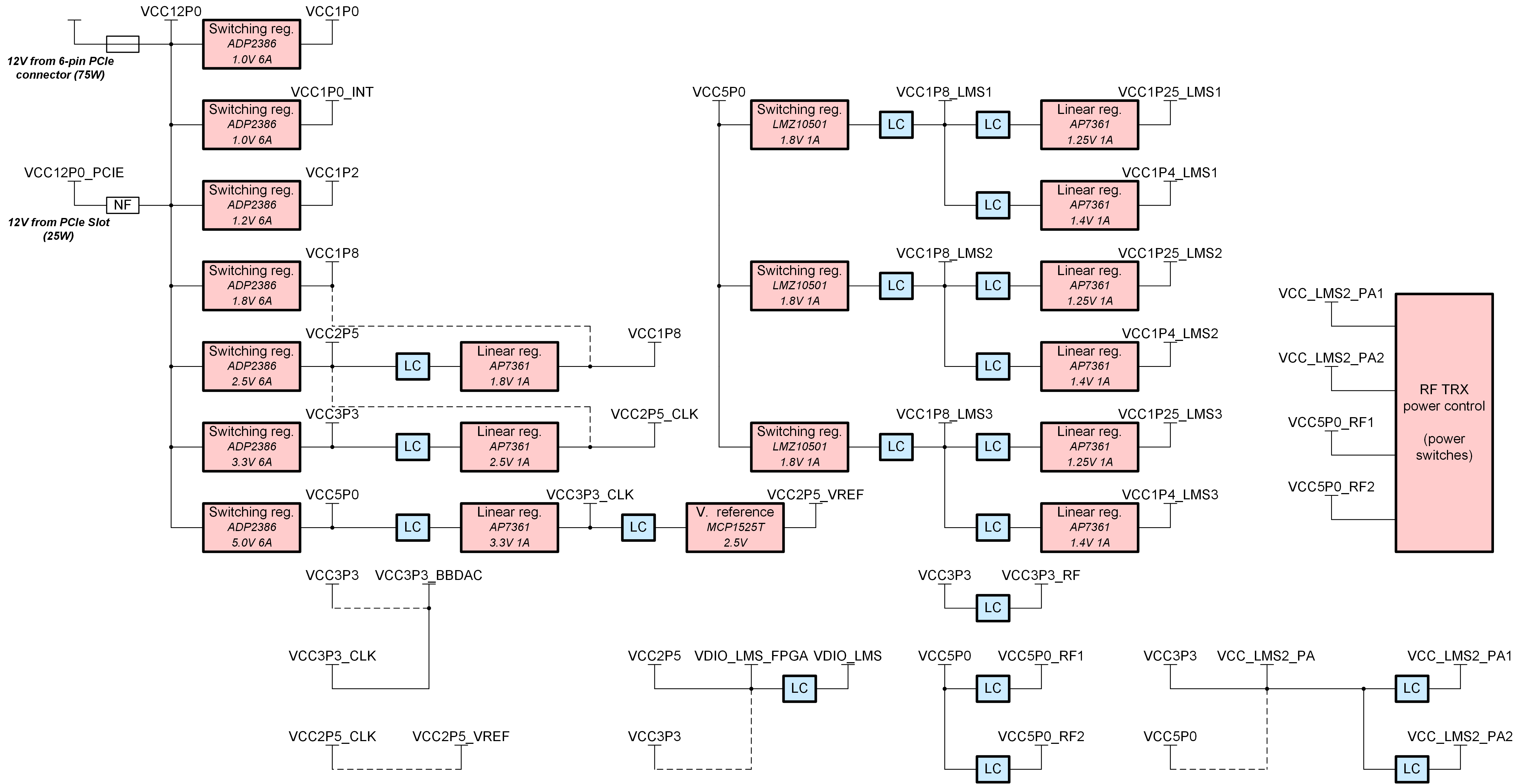
Figure 10. LimeSDR X3 board power distribution diagram